Home
/ Fermi Level In Semiconductor : 1D doped semiconductors / The fermi level is referred to as the electron chemical potential in other contexts.
Fermi Level In Semiconductor : 1D doped semiconductors / The fermi level is referred to as the electron chemical potential in other contexts.
Fermi Level In Semiconductor : 1D doped semiconductors / The fermi level is referred to as the electron chemical potential in other contexts.. Above is a diagram (ref. Due to lack of sufficient energy at 0 kelvin, the fermi level can be considered as the sea of fermions (or electrons) above which no electrons exist. Fermi levels, forward bias prof j. If you can bring the fermi level high enough, then part of the tail will go over to the conduction band. At absolute zero temperature intrinsic semiconductor acts as perfect insulator.
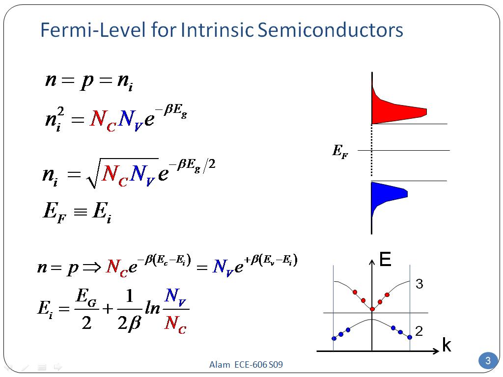
Fermi level, strictly speaking, is defined only when the entire system is in equilibrium. • all energy level in one band is same energy. Such equilibrium can be disturbed by many interactions like shining light, applying a temperature. Fermi level ef to me is the reference level to measure the concentration of electrons or holes in a semiconductor. Fermi level in extrinsic semiconductors in an intrinsic semiconductor at t = 0 the valence bands are filled and the conduction band empty.
nanoHUB.org - Courses: ECE 606: Solid State Devices ... from nanohub.org The fermi level pinning effect is strong in many commercially important semiconductors (si, ge, gaas), and thus can be problematic for the design of semiconductor devices. Due to lack of sufficient energy at 0 kelvin, the fermi level can be considered as the sea of fermions (or electrons) above which no electrons exist. A semiconductor is a solid that is defined as having its fermi level (chemical potential) in a band gap of the electronic structure of the solid, which is not too large compared to the thermal energy, so that, according to the fermi distribution, at room temperature you have a significant number of electrons and/or holes in the conduction and. Ec is the conduction band. At absolute zero temperature intrinsic semiconductor acts as perfect insulator. Of holes in valance band. In a perfect semiconductor (in the absence of impurities/dopants), the fermi level lies close to the middle of the band gap 1. Primer on semiconductors unit 5:
A semiconductor is a solid that is defined as having its fermi level (chemical potential) in a band gap of the electronic structure of the solid, which is not too large compared to the thermal energy, so that, according to the fermi distribution, at room temperature you have a significant number of electrons and/or holes in the conduction and.
Semiconductor doping and higher temperatures can greatly improve the conductivity of the pure semiconductor material. Not an example for intrinsic semiconductor (a) si (b) al (c) ge (d) sn Where the fermi energy is located (correct?). Smith department of eecs university of california, berkeley eecs 105 spring 2004, lecture 19 prof. The fermi level lies between the valence band and conduction band because at absolute zero temperature the electrons are all in the lowest energy state. Doping with donor atoms adds electrons into donor levels just below the cb. The fermi level represents the electron population at energy levels and consequently the conductivity of materials. The fermi energy is defined as: The fermi level concept first made its apparition in the drude model and sommerfeld model, well before the bloch's band theory ever got around semiconductor books agree with the definitions above for fermi level and chemical potential, but would also say that fermi energy means the same thing too. In a perfect semiconductor (in the absence of impurities/dopants), the fermi level lies close to the middle of the band gap 1. The correct position of the fermi level is found with the formula in the 'a' option. The fermi level is referred to as the electron chemical potential in other contexts. Fermi level in extrinsic semiconductors in an intrinsic semiconductor at t = 0 the valence bands are filled and the conduction band empty.
Ec is the conduction band. Fig.2.7.2 graphical solution of the fermi energy based on the general analysis. The fermi energy is defined as: The fermi level concept first made its apparition in the drude model and sommerfeld model, well before the bloch's band theory ever got around semiconductor books agree with the definitions above for fermi level and chemical potential, but would also say that fermi energy means the same thing too. Green, unsw) illustrating the location of the fermi level e f relative to the valence and conduction bands for various materials.
Metal semiconductor junction - Metallization ... from www.halbleiter.org The fermi energy is defined as: The term fermi level is mainly used in discussing the solid state physics of electrons in semiconductors, and a precise usage of this term is necessary to describe band diagrams in devices comprising different materials with different levels of doping. Of electrons in conduction band are greater than no. Fermi levels, forward bias prof j. Green, unsw) illustrating the location of the fermi level e f relative to the valence and conduction bands for various materials. Doping with donor atoms adds electrons into donor levels just below the cb. This is one definition and if we apply concept of fermi level in semiconductors we say it is an energy level between the forbidden band gap (where no electron exists as per the definition) where only the probability is 50%. Not an example for intrinsic semiconductor (a) si (b) al (c) ge (d) sn
Not an example for intrinsic semiconductor (a) si (b) al (c) ge (d) sn
Of free electrons in conduction band. A semiconductor is a solid that is defined as having its fermi level (chemical potential) in a band gap of the electronic structure of the solid, which is not too large compared to the thermal energy, so that, according to the fermi distribution, at room temperature you have a significant number of electrons and/or holes in the conduction and. Ec is the conduction band. Position of fermi level in intrinsic semiconductors • width of conduction band and valence band is small as compared to forbidden energy gap. However as the temperature increases free electrons and holes gets generated. The semiconductor equations lecture 5.3: Kb is the boltzmann constant. Such equilibrium can be disturbed by many interactions like shining light, applying a temperature. • all energy level in one band is same energy. Whenever the system is at the fermi level, the population n is equal to 1/2. The fermi level is at e / u = 1 and k t = u. Fermi level in extrinsic semiconductors in an intrinsic semiconductor at t = 0 the valence bands are filled and the conduction band empty. Due to lack of sufficient energy at 0 kelvin, the fermi level can be considered as the sea of fermions (or electrons) above which no electrons exist.
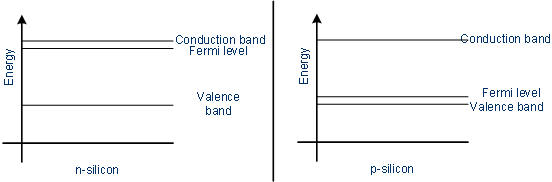
Semiconductor doping and higher temperatures can greatly improve the conductivity of the pure semiconductor material. The semiconductor equations lecture 5.3: Where the fermi energy is located (correct?). The term fermi level is mainly used in discussing the solid state physics of electrons in semiconductors, and a precise usage of this term is necessary to describe band diagrams in devices comprising different materials with different levels of doping. At low t the fermi level lies within the donor levels.
electronic band theory - Where does Fermi level place ... from i.stack.imgur.com Primer on semiconductors unit 5: The fermi level is at e / u = 1 and k t = u. A semiconductor is a solid that is defined as having its fermi level (chemical potential) in a band gap of the electronic structure of the solid, which is not too large compared to the thermal energy, so that, according to the fermi distribution, at room temperature you have a significant number of electrons and/or holes in the conduction and. The fermi level represents the electron population at energy levels and consequently the conductivity of materials. Fig.2.7.2 graphical solution of the fermi energy based on the general analysis. This is one definition and if we apply concept of fermi level in semiconductors we say it is an energy level between the forbidden band gap (where no electron exists as per the definition) where only the probability is 50%. The fermi energy is defined as: The fermi level (i.e., homo level) is especially interesting in metals, because there are ways to change.
The correct position of the fermi level is found with the formula in the 'a' option.
In a perfect semiconductor (in the absence of impurities/dopants), the fermi level lies close to the middle of the band gap 1. Not an example for intrinsic semiconductor (a) si (b) al (c) ge (d) sn The fermi level is at e / u = 1 and k t = u. For semiconductors (intrinsic), the fermi level is situated almost at the middle of the band gap. Fermi level is a kind of measure of equilibrium electronic energy of a solid material. The fermi level pinning effect is strong in many commercially important semiconductors (si, ge, gaas), and thus can be problematic for the design of semiconductor devices. The fermi level represents the electron population at energy levels and consequently the conductivity of materials. A semiconductor is a solid that is defined as having its fermi level (chemical potential) in a band gap of the electronic structure of the solid, which is not too large compared to the thermal energy, so that, according to the fermi distribution, at room temperature you have a significant number of electrons and/or holes in the conduction and. Smith department of eecs university of california, berkeley eecs 105 spring 2004, lecture 19 prof. Position of fermi level in intrinsic semiconductors • width of conduction band and valence band is small as compared to forbidden energy gap. • all energy level in one band is same energy. Such equilibrium can be disturbed by many interactions like shining light, applying a temperature. The fermi level is the level where the probability that an electron occupies the state is 0.5, e.g.
